Abstract
With the rapid expansion of the global electronics industry, the output of electronic waste keeps rising. Countries around the world have introduced solid waste control and circular economy regulations, bringing growing resource constraints and environmental governance pressure. Researchers and industrial practitioners are accelerating the development of treatment processes for electronic waste, focusing on recovering scarce metals such as copper, gold, silver and palladium in waste printed circuit boards (PCBs). In recent years, the industry has summarized the 3R strategy and 4H principles for electronic solid waste resource recovery: Re-manufacture, Reuse, Recycle; High efficiency, High economic benefit, High environmental benefit and High safety performance. PCBs are the carrier of various electronic components. Valuable metals account for a large proportion of the total cost of PCBs. Therefore, efficient resource recovery of waste PCBs has significant potential economic and environmental benefits.
Introduction
Printed circuit boards (PCBs) feature compact structure, high wiring density and stable electrical performance, and are widely used in communication equipment, industrial control instruments, consumer electronics, photovoltaic inverters and other devices. The iteration speed of electronic products keeps accelerating, and a large number of scrapped PCBs enter the solid waste treatment system, bringing great pressure to environmental governance. The waste PCB recycling industry has developed rapidly in recent years. It can reduce the exploitation of primary mineral resources and mitigate environmental risks such as heavy metal leakage and brominated flame retardant pollution. The market prospect is broad with good economic and social benefits. Continuous improvement of the technical system for waste PCB resource recovery is a key research direction in the field of electronic solid waste.
1 Main recovery processes for waste PCBs
PCBs are one of the largest components in e-waste. As the elimination volume of electronic equipment increases, the stock of waste PCBs continues to rise. PCBs are enriched with valuable metals including copper, gold, silver and palladium. Precious metals carry high economic value. However, random landfilling or incineration will release toxic substances such as heavy metals and dioxins, causing long-term harm to soil and water bodies. It is extremely important to develop safe and efficient recycling and regeneration processes for waste PCBs. The existing resource recovery routes for waste PCBs fall into two categories: element recovery and material regeneration. Element recovery: waste PCBs are treated through crushing, separation, leaching and other processes to obtain valuable metal products such as metal salts, metal oxides and crude elemental metals. Material regeneration: while recovering metals, glass fiber and epoxy resin matrix are regenerated to prepare composite materials, adsorbents and other products to realize full-component utilization. Hydrometallurgical leaching is the mainstream route for metal recovery. However, traditional chemical leaching consumes large amounts of reagents with mediocre selectivity, and the leaching rate of some precious metals is relatively low. To solve this problem, researchers have developed bioleaching technology. The metabolic conditions of microorganisms are optimized by adjusting temperature, pH, substrate concentration and other parameters. Under optimal working conditions, the copper leaching rate from PCBs can exceed 90%. Biohydrometallurgy is green and low-toxic. Its application difficulty lies in screening functional strains that can tolerate heavy metals with stable activity. Large-scale cultivation and continuous operation performance still have shortcomings.
2 Recovery of glass fiber and epoxy resin matrix
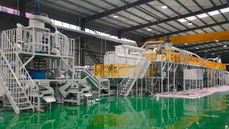
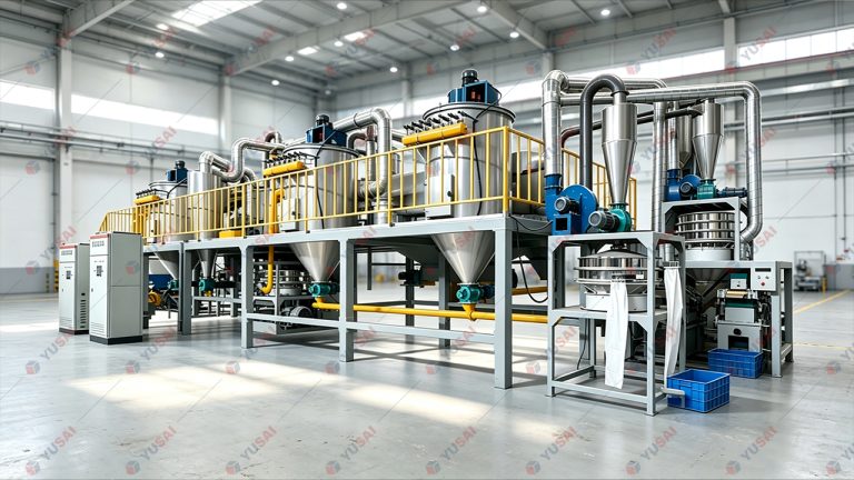
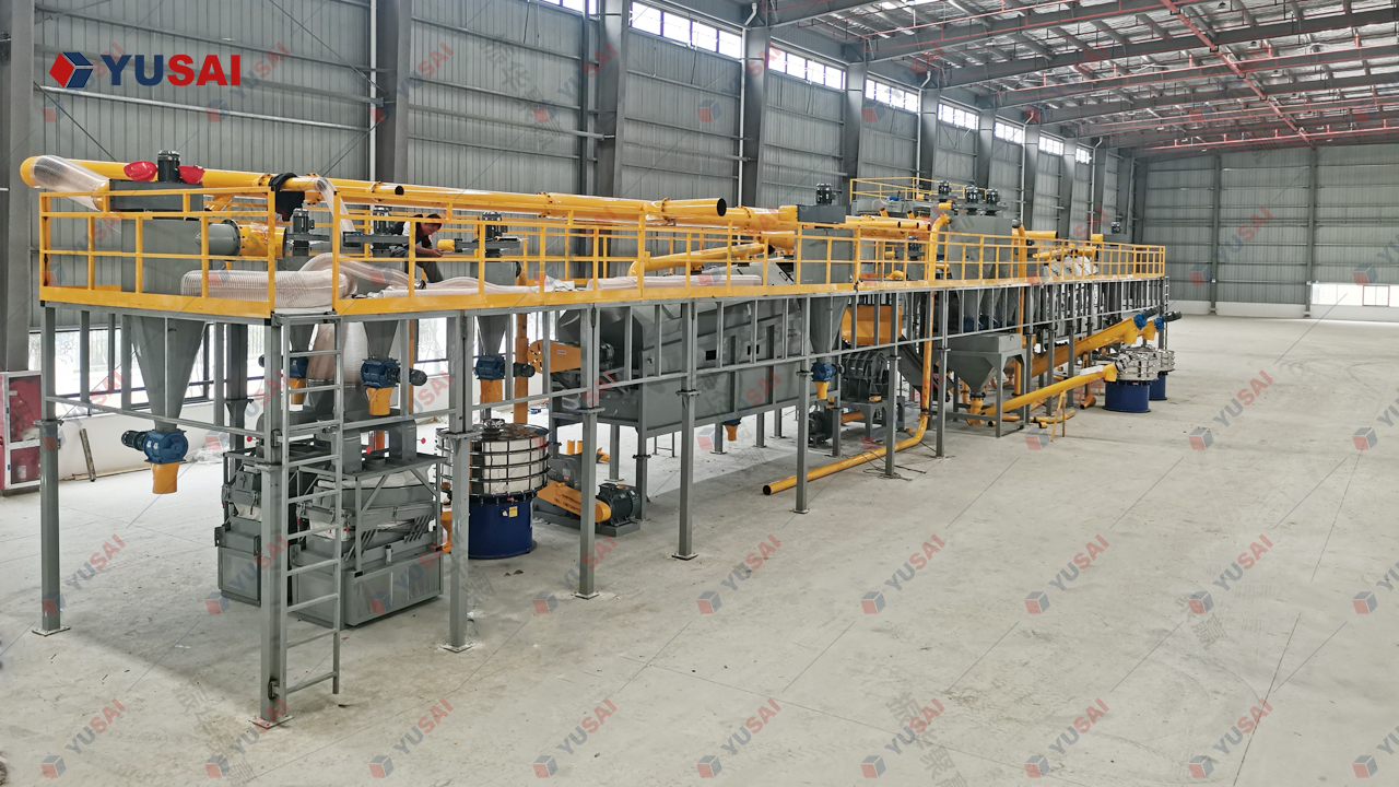
Non-metallic components (epoxy resin + glass fiber) account for 60%~70 wt% of the total mass of waste PCBs. If non-metallic components are only disposed by landfilling, massive resources will be wasted. Meanwhile, brominated flame retardants in resin bring ecological risks. Therefore, resource utilization of PCB non-metallic materials is an indispensable part of a complete recycling process. Regenerated glass fiber can be filled into polymer composite materials and reused as structural fillers in building materials and modified plastic products. At the same time, pyrolysis products of resin can recover fuel oil and combustible gas. The recovered non-metallic powder can not only be used to prepare composite materials, but also be developed into functional adsorption materials for heavy metal adsorption in industrial wastewater and Fenton catalytic systems. Other researchers have modified non-metallic substrates from waste PCBs to prepare adsorbents for efficient capture of heavy metal ions in water. The primary goal of waste PCB pretreatment is to reduce safety risks during disassembly and crushing and inhibit the release of toxic flue gas. First, complete the disassembly of the whole machine, separate connectors, cables, BMS/control chips and other electronic components. These materials can be sorted and recovered separately without entering the subsequent crushing process. For single-board PCBs, components can be directly stripped before crushing. After crushing and dissociation, gravity separation, magnetic separation and electrostatic separation are adopted to separate metal and non-metal mixtures. Fine particles after crushing tend to agglomerate due to epoxy resin bonding, which reduces the accuracy of sorting and separation. Therefore, thermal treatment or chemical debonding is often used before sorting to remove organic bonding phases, break particle agglomeration, improve the separation efficiency of metal and non-metal components, and increase the recovery rate of valuable metals.
Conclusion
In summary, the ownership of electronic equipment in China is huge, and the production of waste PCBs keeps rising. It is necessary to continuously promote the industrial application of waste PCB resource recovery technology and convert electronic waste into renewable resources. Resource utilization of waste PCBs can reduce the whole-chain energy consumption caused by primary mineral mining, cut emissions of heavy metals and persistent organic pollutants, and generate considerable economic and social benefits. Nevertheless, continuous technological innovation is still required for waste PCB resource recovery. At present, some processes are still in the laboratory and pilot scale stage. The stability of continuous production and treatment schemes for waste gas and liquid need further optimization. Relevant enterprises and research institutions should continue research on waste PCB recycling processes, and combine advanced sorting, hydrometallurgy and bio-metallurgy technologies to realize efficient, safe and green resource recovery of waste PCBs.